(Orig Static) CMAC creates a message authentication code from an encryption primitive. The most common is the AES-CMAC, which is described fully in RFC 4493. It involves operating the AES operation in cipher-block chaining mode, where each 16-byte chunk of the original plaintext is fed to the AES encryption operation in turn and combined with the output… Continue reading Summary of AES-CMAC
Power attack on AES-CMAC – the setup
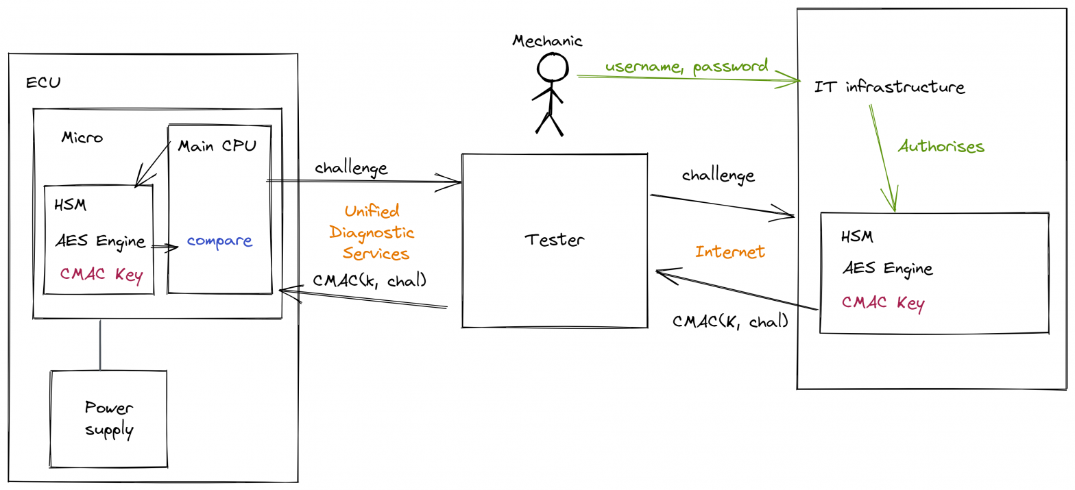
In normal operation, the mechanic uses a piece of equipment which is colloquially known simply ‘a tester’ which talks to the ECU using the ISO-14229 UDS services. Often this is over a CAN-bus but can also be over Flexray, LIN, Ethernet etc. When the mechanic needs to access some secured aspect of the ECU they… Continue reading Power attack on AES-CMAC – the setup
Power side-channel attack on AES-CMAC
AES-CMAC is a popular message authentication code in the automotive world. Although I have been working in automotive electronics for 25 years, I don’t know the actual reason why. But my surmise is that this stems from the fact that the first cryptographic accelerators used in automotive met the “Secure Hardware Extensions” (SHE) specification, which… Continue reading Power side-channel attack on AES-CMAC
RIP Sir Clive Sinclair
A hero of the early home computing era, Sir Clive Sinclair, died on 15th September 2021. Sir Clive was a diverse inventor, way ahead of his time. The portable TV, at the time scoffed at – “you can’t watch TV on the move” – now a commonplace activity. His battery-powered trike was really just waiting… Continue reading RIP Sir Clive Sinclair
ISO/SAE 21434 is ready
This standard for road-vehicles cybersecurity engineering finally sees the light of day. It was developed under both the International Standards Organisation and the Society of Automotive Engineers, after a lot of hard work from many contributors across the industry. The standard gives a framework within which designers of vehicles, and the electronic control units within… Continue reading ISO/SAE 21434 is ready
What is an embedded system?
I just wrote a post for an Infosec site, discussing some definitions of embedded systems. I survey some existing definitions, describe why I don’t feel they represent the current state of embedded systems, and offer another: “It’s an embedded system if the end-user doesn’t control the code that it runs”. Once an end user takes… Continue reading What is an embedded system?
Why use an FPGA?
“Please help me do this on an FPGA” The question you shouldn’t ask! A common refrain on many of the internet’s finest help forums and newsgroups is “I’m trying to do x using an FPGA, help!” And very often “x” is a task which would be more optimally (by many different measures!) be performed in… Continue reading Why use an FPGA?
Flash memory through the ages
I was reading bunnie’s recent post on the manufacturing techniques used in USB flash-drives… bare die manipulated by hand with a stick! Today I found an old (128MB!) SD card from my Palm Tungsten-T. Circa 2005 if I remember rightly. Very different technology, actual chips soldered down on the board. And it’s clear that the… Continue reading Flash memory through the ages
More ARM FPGA
A while ago I compared Altera and Xilinx’s ARM-based FPGA combos. More information is now available publicly, so let’s see what we know now… One thing that’s hard to miss is that Altera are making a big thing of their features to support applications with more taxing reliability and safety requirements. Altera’s external DRAM interface… Continue reading More ARM FPGA
Now running WordPress
This site is now running WordPress, rather then Drupal. Ultimately, I got fed up with the very tedious processes involved with managing a Drupal installation. This added to the fact that I somehow got the Image plugin broken such that I couldn’t upload any more images, and despite much Googling, couldn’t fix it. And this… Continue reading Now running WordPress


